JBL L8400P CLASS-D 600 watt subwoofer amplifier rebuild / PCB rework blog
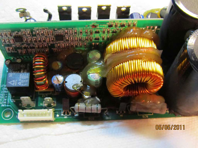
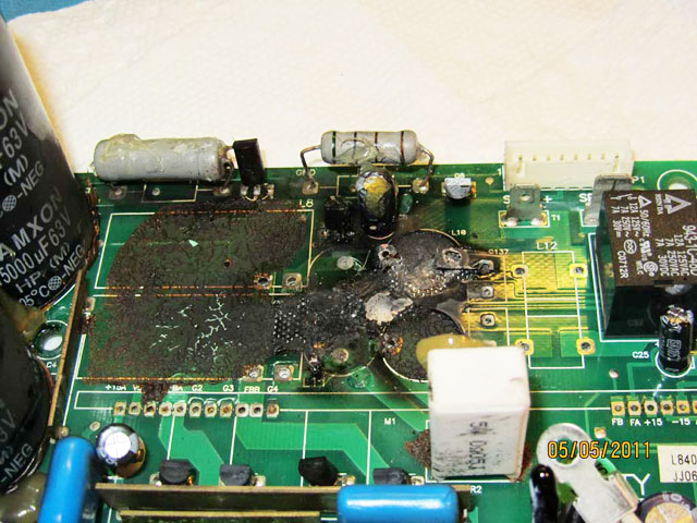
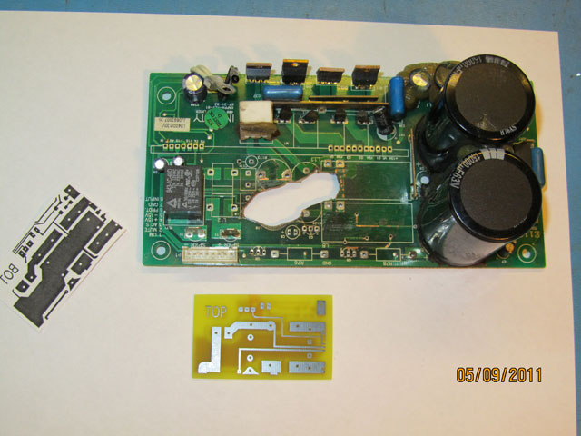
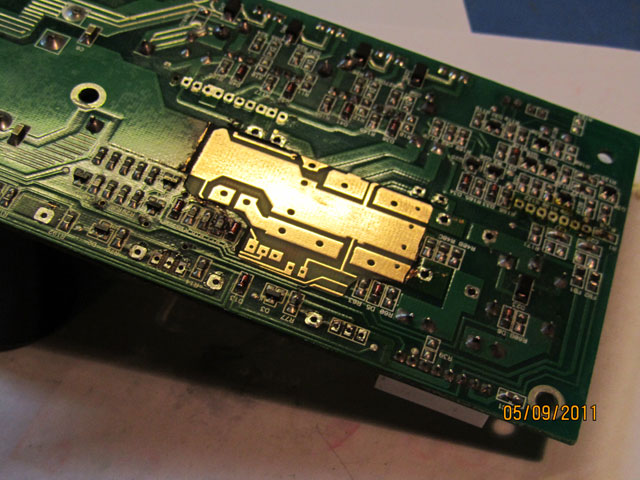
Here is the amplifier after removing from the chassis and before anything has been done. Notice the four bulging capacitors (the reason for the failure).
These capacitors are BIPOLAR electrolytics, and have leaked all over the board where rail voltages were present, causing conductivity to occur and hence flameout of the PCB and surrounding components. After the PCB has burned enough to carbonize, that carbon becomes sufficiently conductive to draw even MORE current, and burn even further, resulting in catastrophic failure, lots of smoke and a NASTY smell!
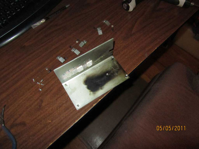
Here you can see the blast mark on the heatsink / chassis where the underside of the PCB assy. was facing. Note the small mass of the heatsink (as CLASS-D amps generally operate at very high efficiencies and do not generate much heat (as compared to the 30-40% efficiencies obtained from similar wattage class A-B amps).
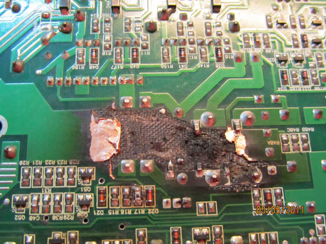
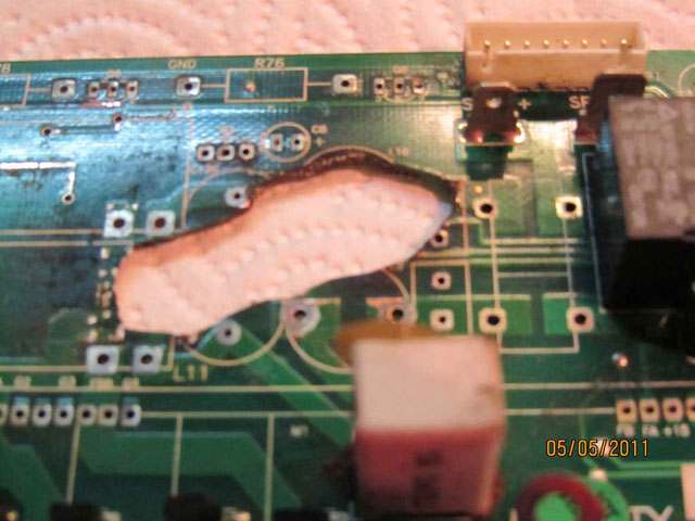
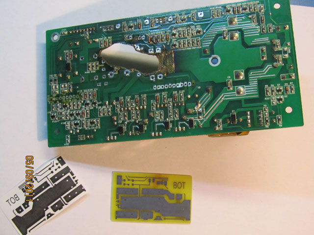
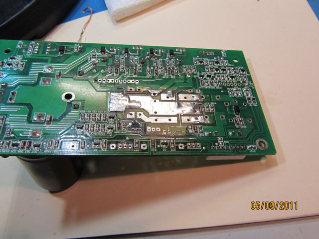
Here you can see the underside of the PCB, after heavy cleaning (with solvent and toothbrush) but before any component removal or rework. Pretty bad huh? Most people would call this board trash. But I LOVE a challenge (and I am not most people ;-)
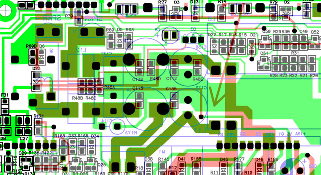
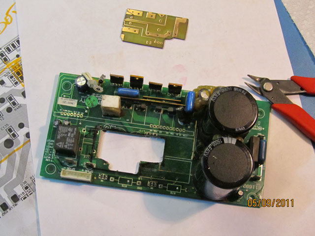
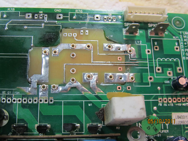
Here is a top view of the PCB after component removal. (Note, that to get through the silicone that held all this together required careful cutting with a retractable razor knife without damaging the components, especially without hitting the enamel on the large toroid inductors)
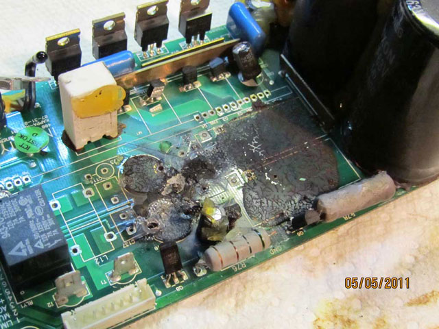
Another angle... UGLY!
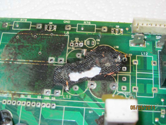
Beginning to clean away the highly conductive carbonized area of the PCB. If you insert leads into any of the blackened areas of this PCB it would read in the low K ohms! (HIGHLY CONDUCTIVE = BAD BAD BAD!)
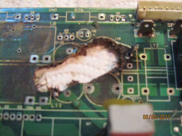
More cleaning... (The center of this hole, where the damage was at it's worst just crumbled out like a charcoal briquette!)
(Top side)
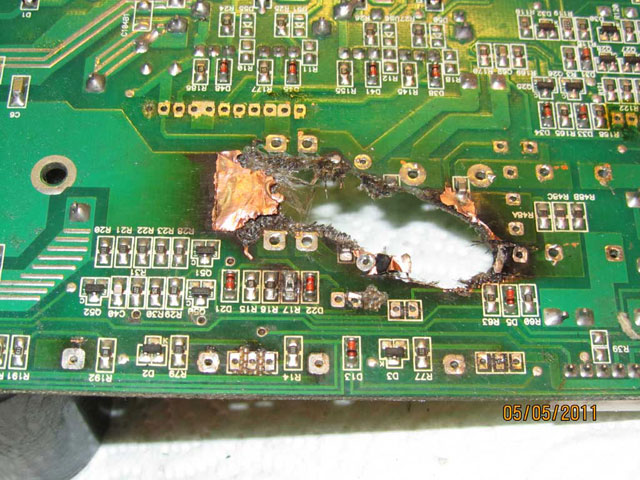
Here the edges have been further cleaned. It is imperative to remove ALL the carbonized areas of the PCB!
Underside (still not there yet...)
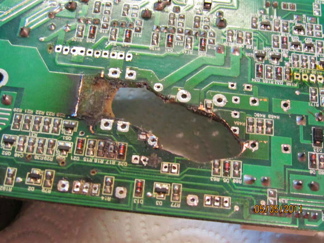
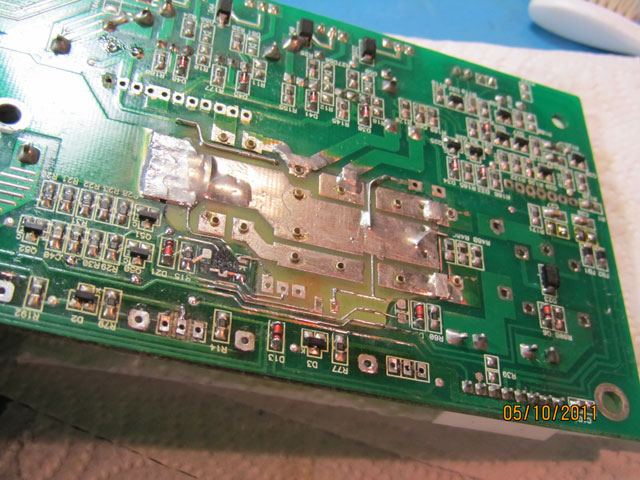
The PCB with mostly all the carbon removed. (I test any suspect areas remaining for resistance just to be absolutely sure!)
The next steps involve making a double sided patch from PCB material of the exact same thickness and copper weight. (I used 2oz copper, and FR4). If you are unsure, use heavier copper, and use calipers to measure the original PCB thickness (on an area with no traces). Since I had the factory service manual for this unit, I was able to do a bit of photoshop magic (after slightly modifying the PDF text to extract the layers and info I wanted, and then importing the reduced result into photoshop).
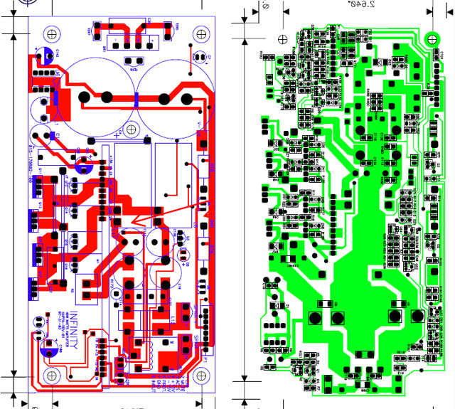
This is what you have to work with from the service manual. It must be reduced to a black and white image of the proper size and contain no information EXCEPT THE COPPER.
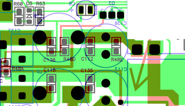
Here are the 2 layers properly aligned and one set to partial transparent (to see them both).
Next, I scanned the actual PCB (with the hole in it), then made a gray transparent area to represent the hole (it is visible if you look close). After aligning the hole using the intact areas of the scanned PCB I have the representation of the damage, all in separate layers and all lined up.
NOTE: The proper sizing had to be achieved (resolution and print size) to make the best result. (I went with 600 DPI) you must have the patch come out EXACT, and this step must be taken beforehand. I achieved it through trial and error until the PDF from the manual was an exact match to the actual PCB after printout.
Then, using the gray area that represents the hole, I determined the optimum patch placement to cover the entire defect. (Note: all of the above images are actually in multiple separate layers in Photoshop. What you see in this blog are flattened JPG's, which are useless for this procedure and are in such format just for the sake of ease of explanation).
Next, trim out all unneeded information, leaving only the copper and label the TOP and BOT layers (so they are identifiable on the final printed patch). What you see here is the flattened result with all layers set to full opacity.

Next run THRESHOLD in Photoshop on each layer, making pure black where any color data was present and pure white where there was none. Now you have your printable patch! Time to go to the heat press...
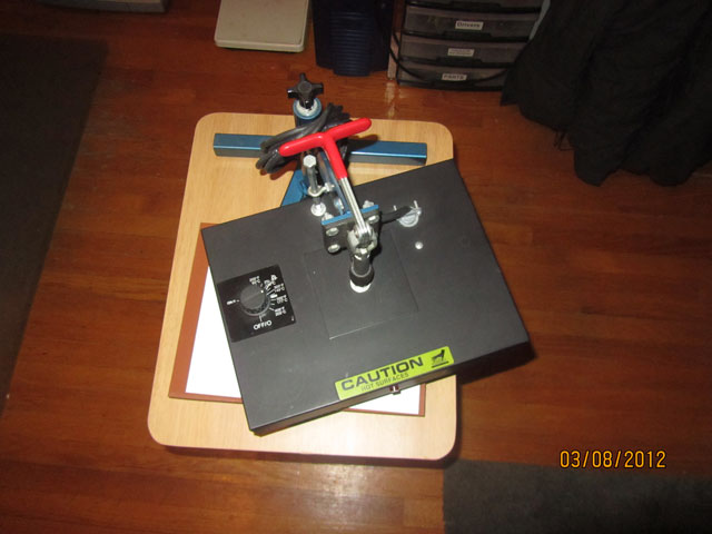
I use this press, but some use laminators with good result. I find keeping the layers accurate and aligned is easier with this type of press. The ability to come straight down, once and clean is important. I use Press-N-Peel blue for all my PCB manufacturing. I have found it to be fairly reliable over the years. I know there are alternative methods, but for graphical PCB work (mainly Photoshop type) I feel this works best for me.
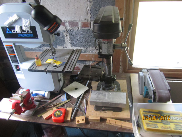
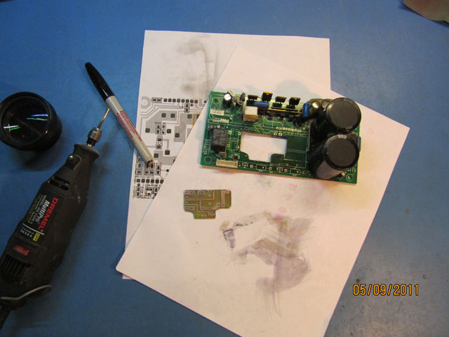
Then it's on to the saw station... If you do this type of work often, then a small bandsaw (with the CORRECT blade) is indispensable! After roughing it out, then I clean up the edges on the belt sander.
Top view of the printed and etched patch (with resist still on).
(Bottom view)
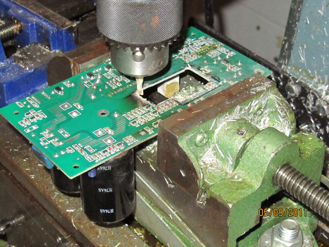
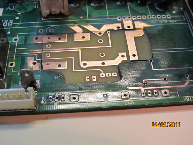
Next, the hole in the PCB needs to be milled out, with clean vertical edges which are cut to logical places with regards to the remaining traces.
Next, the patch gets sanded to an approximate match of the milled hole. This was accomplished by aligning the patch and then tracing through the hole and sanding almost to the traced lines.
Then the final shape is achieved with careful trimming until it fits as perfectly as you can get it.
A good fit!
Everything lines up perfectly!
Perfectly flush with the rest of the PCB.
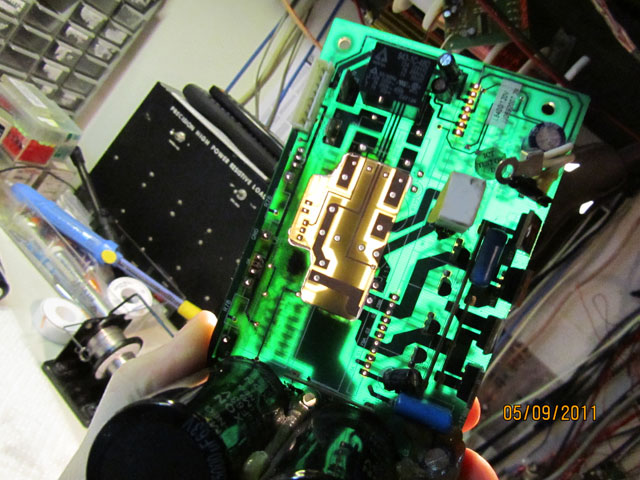
A final check with backlight... Looks good!
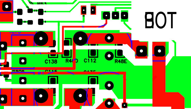
Next the adjacent PCB tracks must be stripped of coating to allow soldering. (Top view)
(Bottom view)
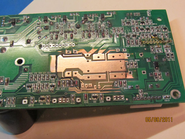
Next begin to connect the traces. Note that solder alone IS NOT SUFFICIENT and WILL FAIL! The gaps here were bridged using solder wick. It is extremely important to keep the profile as low as possible, no huge mountains of solder as it will interfere with the component placement. (Top view)
(Bottom view) Profile height less critical here, but still important. The wick braid is actually visible in this shot where the largest gap was. Unshielded wire was used to patch the finer traces.
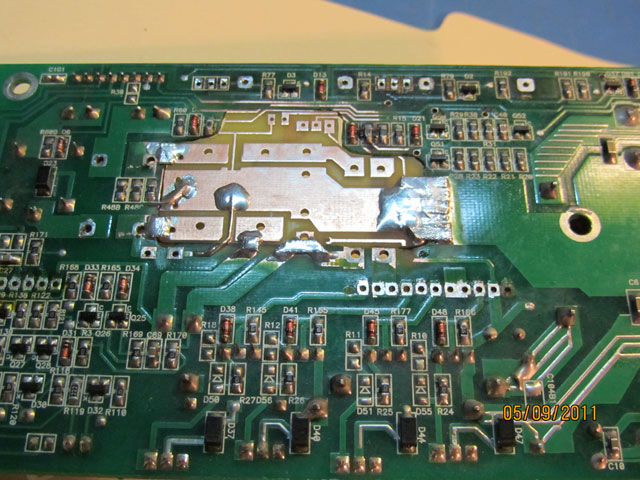
The final patch with all traces bridged, and all exposed copper tinned. (Top view)
(Bottom view)
Next, since the PCB is double sided and the top layer will be completely inaccessible when the components are in place, we need to address the issue of the now missing plated through holes. This was accomplished with the use of grommets. The grommets were soldered into place before component reassembly. (Top view)
(Bottom view) See the slight protrusion of the grommets. (I have a TON of grommets, but no grommet press!) So Just soldering them worked just fine.
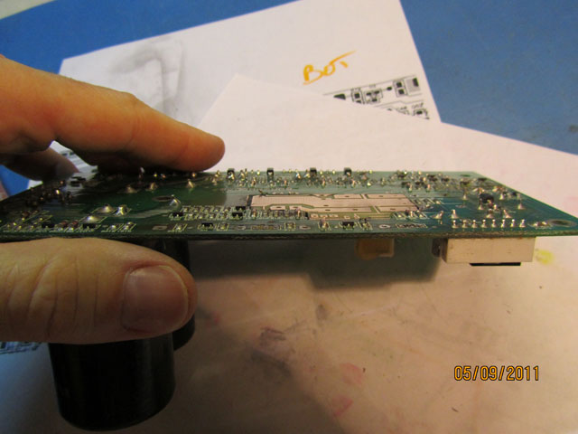
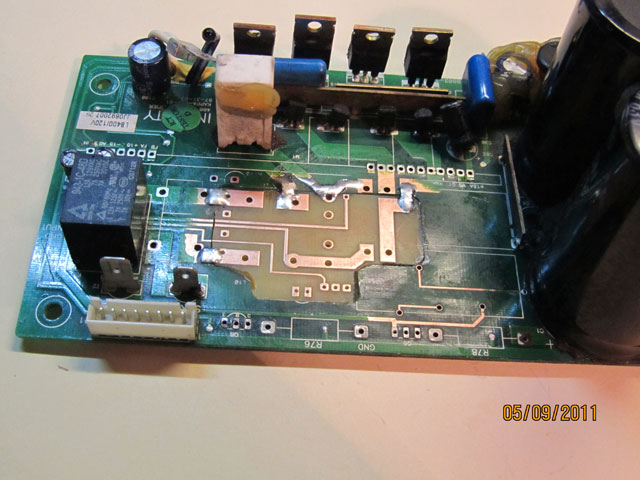
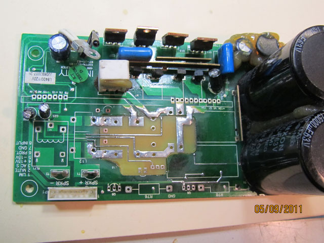
Beginning to reassemble the components. The inferior electrolytic bipolar caps were replaced with polypropylene which will NEVER fail again! Placement is a bit tricky, as these parts are much larger and axial leaded. Leads MUST be kept short as possible to reduce stray inductance and other losses. Q: Why were these parts not used in initial design? A: Because the original parts cost less than $1.00 each. The replacements used here cost about $12.00 each!!! (A MASSIVE cost increase!) (so this repair was over 50$ in caps alone, VS the 4$ in original manufacturer cost parts.) Remember folks... al that matters to the manufacturer is that it will live through it's warranty and nothing else. That is where their responsibility ends.
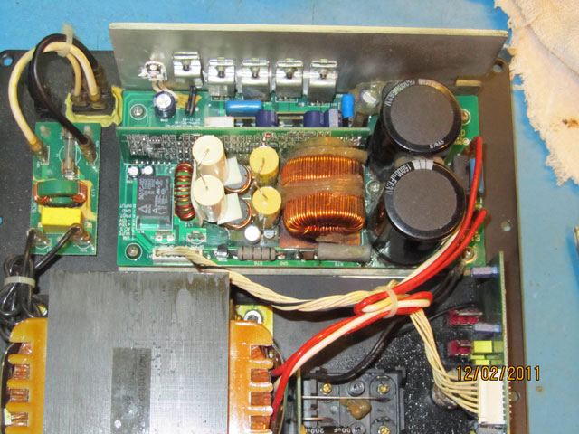
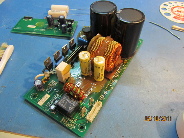
And here is the final result, fully assembled and working. Note the white double-sided 3M foam tape used to secure the components. (Recall, the original assy. was bathed in silicone) Since this is a subwoofer, the entire thing is subject to constant heavy vibration and the need for mechanically securing the components is a must for reliability. I do not like silicone, as it makes rework difficult. The tape is second best to silicone. I was delighted that the unit operated the first time power was applied. Except there was this annoying chirp at power up, which I later found addressed in a service bulletin, so it had to come apart again to fix that, but now it is good to go and should live much longer than the original warranty period!
Thanks for looking! Hope you enjoyed reading this as much as I enjoyed doing it!
You can reach me at xsdb@comcast.net if you have any questions.